
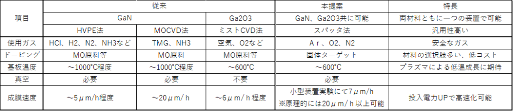
【背景】 近年、現状のシリコン(Si)よりも更に高耐圧・低損失なパワーデバイスの実現が期待できるシリコンカーバイド(SiC)、窒化ガリウム(GaN)といったワイドギャップ半導体材料が注目されています。さらにガリウムの酸化物であるGa2O3は、次世代パワーデバイス用途の新半導体材料としてSiC、GaN同様に優れた材料物性を有しています。パワー半導体の市場は今後大きく伸びていくと予想されています。それぞれの材料の特性を活かした用途に棲み分けされると考えられる。窒化ガリウム、酸化ガリウムにおいては、その薄膜形成方法としては、MOCVD法、HVPE法、ミストCVD法などがあり、それぞれ一長一短があり、国内各社が積極的に研究開発しています。一方で半導体プロセスにおいて広く使われているスパッタ法はこれらの材料の成膜にはほとんど用いられていません。
【目的】 汎用的なスパッタ法にて窒化ガリウムや酸化ガリウムを成膜することで安価で工業的に広く応用できるようにすることで社会に貢献することを目的としています。将来は量産装置の開発まで行いたいと考えています。
【実験/結果】当社では汎用的なスパッタ装置に工夫を施し、窒化ガリウムおよび酸化ガリウムの成膜を行うことに成功しました。現状は小型の装置での実験レベルですが以下のような結果が得られています。またサファイア基板上にはGaNおよびGa2O3がそれぞれエピタキシャル成長をしていることを確認しております。なお成膜方法に関しては新規性が高いため2022年3月に特許出願を行っております。
【今後の方針】 今後、共同で開発を進めてくれる企業様/組織を探しております。ご連絡をいただければ幸いです。
In recent years, wide-gap semiconductor materials such as silicon carbide (SiC) and gallium nitride (GaN) have attracted attention because of their potential to realize power devices with even higher breakdown voltage and lower loss than current silicon (Si). Furthermore, Ga2O3, an oxide of gallium, has excellent material properties as well as SiC and GaN as a new semiconductor material for next-generation power device applications. The market for power semiconductors is expected to grow significantly in the future. It is expected to be segregated into applications that take advantage of the characteristics of each material. For gallium nitride and gallium oxide, the thin film formation methods include MOCVD, HVPE, and mist CVD, each of which has its own advantages and disadvantages, and each company in Japan is actively engaged in research and development. On the other hand, the sputtering method, which is widely used in the semiconductor process, is rarely used for the deposition of these materials.
Our goal is to contribute to society by depositing gallium nitride and gallium oxide by the general-purpose sputtering method, which is inexpensive and can be widely applied industrially. In the future, we hope to develop mass production equipment.
We have successfully deposited gallium nitride and gallium oxide films by applying our ingenuity to general-purpose sputtering equipment. The following results have been obtained, although currently at the experimental level using small equipment. We have also confirmed that GaN and Ga2O3 have grown epitaxially on sapphire substrates. Since the deposition method is highly novel, a patent application will be filed in March 2022.
We are looking for companies/organizations to collaborate with us in the future. We would be happy to hear from you.